Part 1 - System Requirements
When starting a new electronics project, the first step is to define the system capabilities.
These requirements are derived from specific stakeholder needs, whether they are personal, coming from market research, etc…
TL;DR (“too long; didn’t read”)
To start your project you need to define:
- System Description
- 1st Level Requirements Breakdown
- High Level System Block Diagram
- 2nd Level Requirements Breakdown
- Detailed Technical Requirements
- Detailed System Block Diagram
System Description
The System Description serves as the project’s foundation.
In order to define it, identify the following:
-
Functional Intent
“What specific tasks or operations this system needs to perform?”
-
Purpose
“What is the objective or problem this system needs to solve?”
-
Operational Context
“In what environment and for what specific application will this system be used?”
Write down the answer to those questions, consolidate the answers in a formal format and you will end up with your System Description.
Example:
An autonomous, high-speed maze-solving robot designed to navigate a $16 \times 16$ grid, map the environment, and execute the fastest possible path to the center.
This will guide the next design steps.
Requirements Breakdown
After the System Description finalized, decompose the system into several technical specifications.
For example:
- Sensing
- Utilization of high-speed Infrared (IR) emitter-receiver pairs to detect wall proximity and alignment without physical contact.
- Locomotion
- High-RPM brushed or brushless DC motors with high-resolution magnetic encoders for precise sub-millimeter positioning.
- Processing
- Implementation of a “Flood-Fill” or similar pathfinding algorithm to solve the maze in real-time while maintaining high-speed stability.
- Connectivity
- Removable Wireless Telemetry for testing
- Power Source
- Battery powered
System Block Diagram
Draw a high-level diagram representing the different system components as well as their signal and power connections.
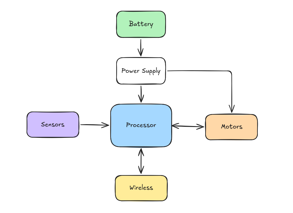 System Block Diagram Example
Detailed Design Specifications
Go through each high-level requirements and break them down further in smaller engineering targets.
Connectivity
When having connectivity requirements like USB or other communication channels, try to determine through educated guess and calculations the necessary bandwidth of data you will need for your application based on other requirements (sensor poll rate and sensor data size, etc…) in order to better determine what will be the bandwidth requirements for your communication channel.
Example:
If your application need sampling like ADC measurement. Use the Nyquist Frequency to determine the sampling frequency requirement. Hence the sampling rate should be at least twice as fast as the frequency of interest. https://en.wikipedia.org/wiki/Nyquist_frequency. To reduce quantisation error and get accurate reading ADC should have a bit depth from 8 to 24 bits, for example 12 is correct. Given your ADC bit depth and your sampling rate you can calculate your data rate: Single channel data-rate: 1 Channel x 12 bits x 40,000 samples per second = 0.46Mbit/s
Example:
- USB
- USB type: 1/2/3 (depends on your data bandwidth need, USB2.0 FS(Full Speed) is up to 12 Mbit/s and HS(High Speed) up to 480Mbit/s)
- Host/Device or Both (On-The-Go OTG)
- Connector: A/B/Mini/Micro/C
- Wireless chip
- Removable -> dev board with connector? (example: ESP-Hosted on ESPx board (Seeed Studio XIAO ESP32-C6), Custom cyw43 board )
- WiFi/Bluetooth
Note:
// TODO: improve this section
Do not forget to add ESD protection to all your connectors headers. ESD can easily damage your components.
Debugging Interace
// TODO: improve
- SWD(Serial Wire Debug) or JTAG(Joint Test Action Group)
Processor
- Brand
- STM32 is recommended
- Number of cores
- Clock speed
- Depends on necessary processing power
- Peripherals
- List down the requirements
- USB, SPI, CAN, …
- Packaging
- Avoid BGA and QFN to reduce cost
- Programming
- Debugging
- SWD(Serial Wire Debug) or JTAG(Joint Test Action Group)
Power Management
Source
USB
When using USB you will need to select the power delivery you need for your circuit. USB-C can negotiate the power it can deliver.
Input power from USB power rail is very noisy. needs adequate filtering. It has nominal +5V but can drop as low as 4.5V. Needs to watch out for regulator drop-out voltages. Can get to 500mA max current if negotiated with host. 150mA otherwise.
Battery
- Cell Type
- Primary (Non-Rechargeable)
- Secondary (Rechargeable)
- Cell Chemistry
- Lithium Ion (Li-Ion)
- 4.2V Charge
- 3.6V Nominal
- 2.5V End-Of-Discharge
- Most Energy Dense
- Most Volatile (Subject to thermal runaway, dendrite growth)
- Lithium Iron Phosphate (LiFePO4)
- 3.65V Charge
- 3.2V Nominal
- 2.0V End-Of-Discharge
- Less Energy Dense
- Less Volatile, hense safer (Not subject to thermal runaway neither dendrite growth)
- Nickel Metal Hydride (NIHM)
- 1.5V Charge
- 1.3-1.2V Nominal
- 1.0V End-Of-Discharge
- Usually used to replace AA (Alkaline non rechargeable)
- Lithium Ion (Li-Ion)
- Cell shape
- Cylindrical
- Better output current
- Sizes: 18650, 21700, 26650
- CID/PTC protection
- Prismatic
- Size: 103450, but usually custom and very large
- Pouch
- Lighter
- No standard size, but flat and usually smaller
- Subject to swelling (they will swell to 20% during their life)
- Cannot tolerate Physical abuse
- Cylindrical
- Number of cells (1S, 2S, …)
- Discharge rate/C-Rate
- Connector type
- Bare Cell (not recommended if you dont have a good protection circuit)
- JST-XH/SYP (3A rating)
- XT30 (higher current rating 30A)
- Cells topology
- Series (more voltage)
- Parallel (more current)
- Tested Batteries with certification
- Do you need to charge the battery? -> need charging circuit/IC
- Example: BQ24109 + 3V3 Buck Boost
- Battery Safety/Protection circuit
- It can come integrated with the battery pack (Pouch or Cylindrical), and is recommended
- Needed on the PCB if use bare cells with cell holder. Not recommended.
- Placed just after the battery connection (before the load/charger)
- Protects the battery from the load/charger
- Safety features
- Over Voltage Protection (OVP)
- Protects the battery from being charged past the peak charge voltage
- Under Voltage Protection (UVP)
- Protects teh battery from being depleted past the End-Of-Discharge voltage
- Over Current In-Discharge (OCD)
- Prevents the load from drawing too much discharge current
- Over Current In-Charge (OCC)
- Prvents the charger from providing too much charge current
- Over Temperature Protection (OTP)
- Cuts off battery output when the temperature is too high
- Short Circuit
- Cuts off battery output during a short on the battery output
- Over Voltage Protection (OVP)
- Example
- “Non Smart” IC, hardcoded protection values
- 1 cell R5480K261CL
- 2 cells R5460M208AF
- “Non Smart” IC, hardcoded protection values
Regulation
- Need different ones?
- Switching/Linear
- Digital: switching supply (buck converter) for efficiency. Digital is more tolerant of noise. Simple digital circuitry draws 100s of mAs.
- Analogue: Linear (LDO) regulators for improved noise reduction if the analogue circuit is for sensing. Analogue sensing circuitry usually draws less current than digital (10s of mAs).
Mechanical Requirement
- PCB dimension constraints (//TODO:)
- Mounting holes (grounded?)
- Connector placement
- Which case are we designing for? (conductor?)
Peripherals Requirements
- LED to indicate power on
- LEDs connected to MCU for status information
Other requirements
- Timing (crystal frequencies, types, etc..)
- ESD protection and filtering for EMC
Detailed System Block Diagram
Combine all previous requirements to draw a detailed system block diagram.
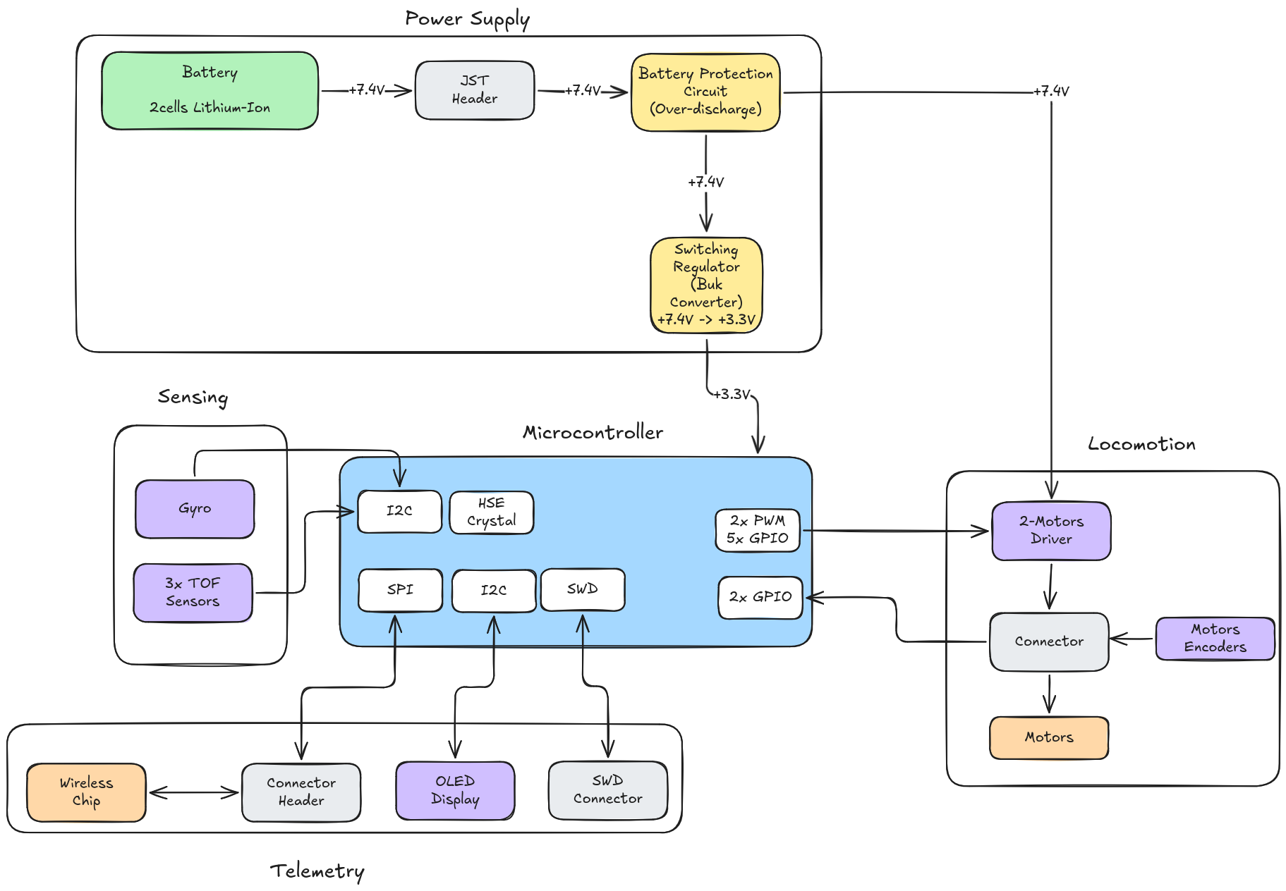 Detailed System Block Diagram Example